Students can Download 2nd PUC Electronics Chapter 3 Transistor Amplifiers Questions and Answers, Notes Pdf, 2nd PUC Electronics Question Bank with Answers helps you to revise the complete Karnataka State Board Syllabus and score more marks in your examinations.
Karnataka 2nd PUC Electronics Question Bank Chapter 3 Transistor Amplifiers
2nd PUC Electronics Transistor Amplifiers One Mark Questions and Answers
Question 1.
What is an amplifier?
Answer:
Amplifier is a circuit which increases the strenght of weak input signal without any change in its shape.
Question 2.
What is faithful amplification?
Answer:
Faithful amplification is the process of increasing the strength of the signal without any change in its shape.
Question 3.
What are the functions of input and output coupling capacitors?
Answer:
The coupling capacitors block dC and allow ac signal.
Question 4.
What is the phase difference between input and output in CB amplifier?
Answer:
0°
![]()
Question 5.
What is the phase difference between input and output in CE amplifier?
Answer:
180o
Question 6.
What is the phase difference between input and output in CC amplifier?
Answer:
0C
Question 7.
Which of the three types of amplifiers is best suited for low input impedance and high output impedance?
Answer:
CB amplifier.
Question 8.
What is operating point?
Answer:
The zero signal collector current and collector to emitter voltage is called operating point.
Question 9.
Why does base collector junction get heated more than the emitter base junction in a common emitter amplifier?
Answer:
The collector current is more than base current and collector base junction has more resistance as it is reverse biased. Hence collector base junction gets heated more.
Question 10.
Which transistor amplifier produces maximum current gain, voltage gain and power gain?
Answer:
Common emitter amplifier.
![]()
Question 11.
Why is a CC amplifier called as emitter follower?
Answer:
CC amplifier is called emitter follower because the emitter voltage follows the base voltage.
Question 12.
Why does a transformer coupled amplifier give poor frequency response?
Answer:
The disproportionate amplification of frequencies in complete signals the reason for poor frequency response.
Question 13.
Why is transformer coupled amplifier used in the final stage of multistage amplifier?
Answer:
For impedance matching and maximum output.
Question 14.
What is the use of a bypass capacitor in CE amplifier?
Answer:
The emitter by pass capacitor bypasses the alternating current at the emitter to the ground by provinding easy alternate path.
Question 15.
What is the use of RE in CE amplifier?
Answer:
The resistor RE provides the stabilisation of the operating point.
Question 16.
What happens to base current when emitter base junction is reverse biased in CB
amplifier?
Answer:
Base current decreases.
Question 17.
What is buffer amplifier?
Answer:
Buffer amplifier is an amplifier with unit gain which is used to deliver the maximum power to the load.
Question 18.
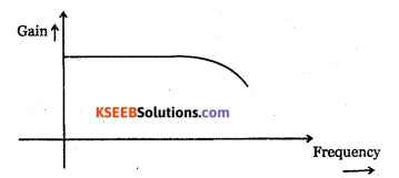
What is meant by frequency response of an amplifier?
Answer:
The variation of the gain of an amplifier with the frequency of the input signal is called frequency response of the amplifier.
![]()
Question 19.
What is a power amplifier?
Answer:
Power amplifiers are used to boost the power level of the input signal.
Question 20.
What type of amplifier is used to drive the loud speaker system of a record player?
Answer:
CC amplifier.
Question 21.
How do you classify the power amplifier based on the position of operating point?
Answer:
- Class A
- Class B
- Class AB
- Class C
Question 22.
Write the expression for the efficiency of power amplifier?
Answer:
Efficient,\({ n }=\frac { { { P }_{ out({ a }{ c }) }\quad } }{ { P }_{ { in }({ d }{ c }) } }\)
2nd PUC Electronics Transistor Amplifiers Two Marks Questions and Answers
Question 1.
Mention the biasing conditions for normal operation of a transistor amplifier?
Answer:
- The operating point should be at the centre of load line.
- Collector current should be kept constant against temperature variations.
- The operating point should not change when transistor is replaced by another of same type.
Question 2.
Why do we prefer to express the gain in decibel?
Answer:
- Loudness heard by human ear is according to the logarithm of the intensity of sound.
- In multistage amplifiers, total gain in decibel is equal to the sum of the decibel gains of individual stages.
![]()
Question 3.
A CC amplifier does not produce any voltage gain. Explain.
Answer:
In CC amplifier, voltage gain =
Question 4.
Mention alternate names for CC, CB and CE amplifiers?
Answer:
CC amplifier = Emitter follower, Buffer amplifier.
CB amplifier = Radio frequency amplifier.
CE amplifier = Audio frequency amplifier.
Question 5.
How CE amplifier can produce 180° phase shift?
Answer:
Output voltage VCE = VCC – ICRC. During positive half cycle forward bias increases. Hence IC increases and as Icc is constant, VCE decreases.
Question 6.
Write the steps involved in drawing AC equivalent circuit af an amplifier.
Answer:
- Replace DC sources by short circuit.
- Replace capacitors by short circuit.
Question 7.
Draw AC equivalent circuit diagram of a single stage CE amplifier.
Answer:
Question 8.
Draw DC equivalent circuit diagram of single stage CE amplifier.
Answer:
Question 9.
Write the steps involved in drawing DC equivalent circuit of an amplifier.
Answer:
- Reduce all the AC sources to zero.
- open all the capacitors.
![]()
Question 10.
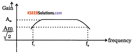
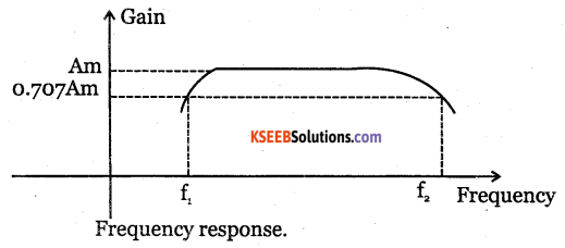
Why do we consider frequencies above 70.7% of the maximum gain for bandwidth?
Answer:
If the gain falls to 70.7% of maximum gain, the ear can not detect the change in the intensity of sound. If the gain falls below 70.7%, the ear will hear distortion. Hence the range of frequencies above 70.7% of the maximum gain is called as bandwidth.
Question 11.
Why do we avoid RC and transformer coupling for very high and very low frequencies?
Answer:
Since reactance (XL and Xc) depend on frequency, RC and transformer coupling is avoided for very high and low frequencies.
Question 12.
Explain the functions of the coupling and bypass capacitors?
Answer:
Coupling capacitors are used to block dc and allow only ac to pass through. The emitter bypass capacitor bypasses the alternating current at the emitter to the ground by providing easy alternate path.
Question 13.
Draw the frequency response of CE amplifier.
Answer:
Question 14.
Mention two characteristics of a CC amplifier.
Answer:
- Voltage gain is nearly equal to 1.
- Input and output signals are in phase.
Question 15.
Why does the gain of an amplifier decrease at very low and very high frequencies?
Answer:
The capacitive reactance of coupling and by pass capacitors is large at low frequencies. As this reactance with is in series with source resistance, the input signal is attenuated and the gain is less.
![]()
At high frequencies, the reactance offered by junction capacitance of transistor and wiring capacitance is less. As this is in paralled with output resistance, gain decreases with increase in frequency.
Question 16.
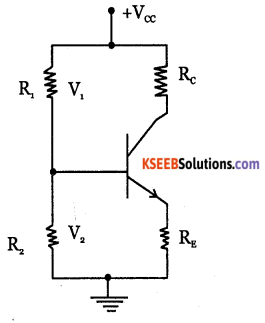
Draw the circuit of a CB amplifier?
Answer:
Question 17.
Why docs a transformer-coupled amplifier produce humming noise?
Answer:
Magnetostriction (extension and contraction of magnetic sheet steel when magnetised) is the reason for noise in transformer-coupled amplifier.
Question 18.
What are the disadvantages of a direct-coupled amplifier?
Answer:
- High frequency signals cannot be amplified.
- It has poor temperature stability.
Question 19.
What are the advantages of an RC coupled amplifier?
Answer:
- Distortion is minimum.
- Overall gain is high.
- It has good frequency response.
- It costs less.
Question 20.
Write any two applications of CC amplifier?
Answer:
- CC amplifier is used as buffer amplifier to deliver maximum power to the load.
- It is used as current amplifier
Question 21.
What is the necessity of cascading?
Answer:
Cascading of amplifiers is required to get high overall gain.
![]()
Question 22.
What are the functions of power amplifier?
Answer:
Power amplifiers drive the loud speakers in audio systems, radio and TV receivers.
Question 23.
Write a note on cross over distortion in a power amplifier?
Answer:
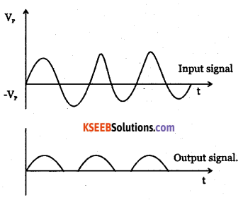
The transistor does not conduct until the input signal voltage exceeds 0.7V for silicon and 3V for Germanium. Due to this, there is time interval between positive and negative cycles of input signal. The distortion when neither of transistors is conducting in push pull amplifier is called cross over distortion.
Question 24.
Distinguish between power amplifier and voltage amplifier?
Answer:
Power amplifiers are used to increase the power level of the input signal. Voltage amplifiers are the amplifiers that amplify small input signals whose amplitudes are very much smaller than DC operating point value.
2nd PUC Electronics Transistor Amplifiers Three Marks Questions and Answers
Question 1.
With a circuit diagram, explain how a transistor can amplify a signal OR Explain the principle of amplification.
Answer:
During positive half cycle of ac input signal, the forward bias on the base emitter junction increases. Hence iB and ic increase and voltage drop across Rc increases. As VCE = Vcc – icRc we get negative half cycle amplified at the output.
During negative half cycle of ac input signal, forward bias on the base emitter junction decreases. Due to this iB and ic decrease and voltage drop across Rc decreases.
AS VCE = Vcc – icRc We get amplified positive half cycle at the output.
![]()
Question 2.
What is cascaded amplifier? Why is it necessary?
Answer:
Cascaded amplifier is number of amplifiers connected in series. Cascading of amplifiers is required to get high gain.
Question 3.
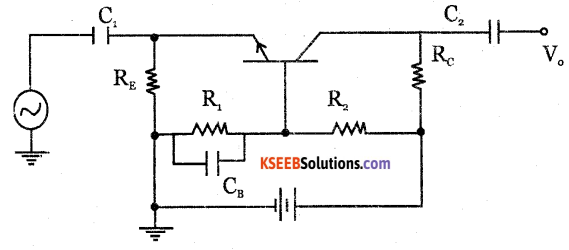
With circuit diagram, explain working of CB amplifier?
Answer:
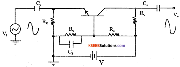
The voltage divider biasing is used biasing CB amplifier. Emitter base junction is forward biased by voltage across R, and the collector base junction is reverse biased by the voltage across Rr Coupling capacitors block DC and allow AC to pass through. By pass capacitor CB by passes AC.
During positive half cycle of input signal, forward bias on the base emitter junction decreases as it is reverse biased,Hence Ic and ICRC is decreased.The output voltage VCB is increased because VCB = Vcc – ICRC. Thus positive half cycle is obtained at the output.
During negative half cycle of the input signal, forward bias on base emitter junction is increased. Hence IE, and Ic increase and IC,RC also increases. As VCB = Vcc – IcRr, VCB decreases as LRr increases. Thus negative half cycle of output is obtained. The input and output signals are in phase.
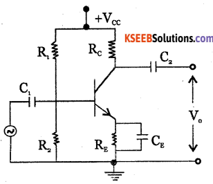
Question 4.
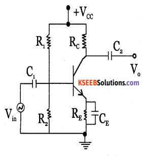
With circuit diagram, explain the working of CE amplifier?
Answer:
The ac signal is applied between base and emitter terminals and output is taken at the collector. R1, R2 provide biasing to the transistor. R1 provides stabilisation and CF provides easy alternate path for the ac to flow, coupling capacitors C1 and C2 block DC and allow ac signals.
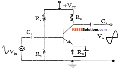
During the positive half cycle of input signal, forward bias emitter base junction increases. Hence base current IB, IE and Ic increase. This makes ICRC increase. Output voltage VCP is given by VCE = Vcc – ICRC. As ICRC increases, VCE decreases and negative half cycle at the output is obtained.
During the negative half cycle of ac input signal, forward bias on emitter base junction
decreases. Hence IB, Ic and IE decrease, decreasing ICRC.
The output voltage VCE = Vcc – ICRC. As ICRC decreases, VCE increases and we get positive half cycle at the output. Thus there is a phase difference of 180° between the input and voltage.
![]()
Question 5.
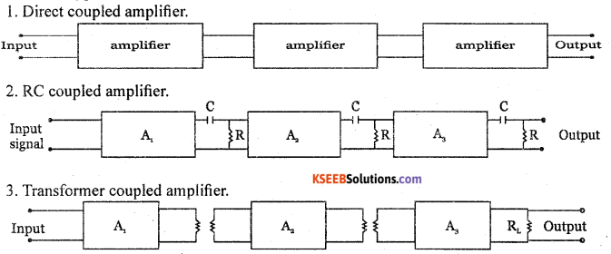
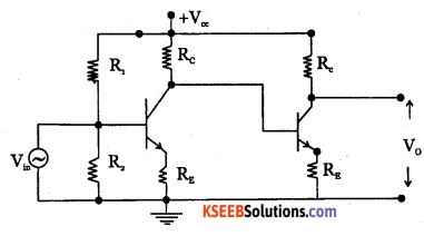
Mention types of coupling of amplifier with block diagrams.
Answer:
Question 6.
Compare different types of coupling of amplifiers?
Answer:
| Parameter | RC coupling | Transformer coupling | Direct coupling |
| Frequency Response |
Excellent | Poor | Best |
| Cost | Less | more | least |
| Weight | Less | more | least |
| Impedance matching |
Not good | Excellent | Good |
| uses | For voltage amplification | For power amplification | For amplifying very low frequencies. |
Question 7.
Define Class A, Class B, Class C power amplifiers.
Answer:
- Class A power amplifier: The Q point is located exactly at the centre of the load line. The current flows for full cycle of input signal.
- Class B power amplifier: The Q point is located in between X-axis and the centre of load line. The output current flows for more than half cycle and less than full cycle of the input signal.
- Class C power amplifier: The Q point is located beyond cut off region below the X-axis. The output current flows for less than half cycle of input signal.
Question 8.
Which of the power amplifiers amongst Class A, Class B or Class C produce maximum distortion? Which is more suitable for faithful amplification? Where is Q point fixed in the case of class AB amplifier?
Answer:
Class A is more suitable for faithful amplification. Class C power amplifier produces maximum. distortion. In Class AB amplifier, Q point is located in between X-axis and the centre of load line.
Question 9.
Which of the Class A, Class B or Class C power amplifiers have maximum efficiency? Mention approximate power efficiency of these amplifiers.
Answer:
Class C power amplifier has maximum efficiency.
| Class | Efficiency |
| A | 25 to 30% |
| B | 70 to 80% |
| C | Higher than 80% |
| AB | 50-70% |
Question 10.
Write one application each for CB, CC, and CE amplifiers.
Answer:
| Amplifier | Application |
| CB | RF amplification |
| CE | AF amplification |
| CC | Impedance matching |
![]()
Question 11.
Explain the working of a CC amplifier?
Answer:
The circuit of a single stage common collector amplifier using npn transistor is shown below:
The ac is applied between base and collector terminals collector circuit. The collector of the transistor is at ac ground as Rc = 0 Vcc, R1,R2,RE provide voltage divider DC bias with constant operating point in the active region. The output is taken across the emitter resistor RE. C, and C2 are the coupling Capacitors which block DC and allow ac signal.
During positive half cycle of input signal, forward bias on emitter base junction increases. Hence the base current emitter current and IERE increases which is output voltage. Hence we get positive half cycle at the output.
During negative half cycle, forward bias between emitter base junction decreases. Hence, IB, IE and IeRe decrease which is the output voltage. Thus negative half cycle is obtained. The input and out signals are in phase. CC amplifier is also called emitter follower because emitter voltage follows the base voltage.
Vo= IERE = Vin -VBP
Vo = Vin -VBP is very small
∴ Vo ≈Vin
Voltage gain
\(A_{V}=\frac{V_{o}}{V_{i n}}=1\)
CC amplifier is used as impedance matching device.
Question 12.
Explain the working of direct coupled amplifier.
Answer:
The direct coupled amplifier using two npn transistors is as shown in the diagram. In this method, output of first stage is directly coupled to the input of second stage. Resistors R1 and R2 form voltage divider circuit. Any signal at the base of the first transistor is amplified A, times and appears at the collector of first stage.
![]()
It is then applied to the base of transistor in the second stage. Hence it is amplified A2 times. The gain of the direct coupled amplifier is A = A x A . Direct-coupled amplifiers are used to amplify extremely low frequency signals.
Frequency Response of Direct coupled transistor amplifier.
Question 13.
Explain the working of RC coupled amplifier.
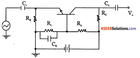
Answer:
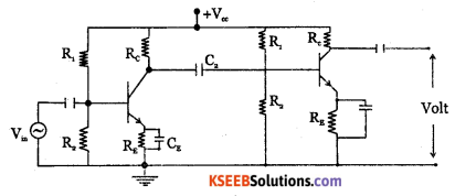
RC coupling is most widely used method of coupling signal from one stage to next stage in multistage amplifiers. The two stage RC coupled amplifier is as shown in the diagram. The signal developed across the collector resistor Rc of the first stage is capacitively coupled to the input of second stage through the coupling capacitor Cc.
RC coupled transistor amplifier is widely used as it provides excellent audio fidelity over wide range of frequency.
R1R2,Rc,RE provide biasing resistors. RE provides stabilisation and CE is used for bypassing ac across Rg.
Working:
When an AC signal is applied to the input of first stage, it gets amplified and appears at its output with a phase reversal of 180°. Through the coupling capacitor Cc, the amplified signal is fed to the input of second stage.
Cc blocks DC and allows AC to pass through. The second stage further amplifies the signal, further providing a phase reversal of 180° with respect to its input. The input and output signal are in phase as the signal is reversed twice. Overall gain of RC coupled amplifier is the product of gain of individual stages.
At low frequencies, reactance of coupling capacitor is high. Hence it allows only a small part of the signal to pass from one stage to next stage. Hence gain is low at low frequencies. At high frequencies, the coupling capacitor Cc offers low reactance and acts like a short. Hence loading effect of next stage increases and the gain decreases.
In mid frequency range, as frequency increases, the capacitive reactance of coupling capacitor decreases, which tries to increase gain. As capacitive reactance decreases, due to loading effect of next stage, the gain reduces. Hence, voltage gain is constant.
2nd PUC Electronics Transistor Amplifiers Five Marks Questions and Answers
Question 1.
Classify amplifiers on different criteria.
Answer:
| Criteria | Classification. |
| 1. Input signal | i. Small signal amplifier, large amplifier |
| 2. Nature of output | i. Voltage amplifier. ii. Power amplifier. |
| 3. Frequency range | i. AF amplifier ii. RF amplifier iii. IF amplifier iv. VHF amplifier v. UHF amplifier vi. SHF amplifier |
| 4. Operating point | Class A Class B Class C Class AB |
| 5. Configuration. | CB amplifier CE amplifier CC amplifier |
| 6. Coupling. | RC coupled Direct coupled Transformer coupled |
| 7. Stages. | Single stage. Multistage |
| 8. Bandwidth | Wideband amplifiers. Narrow band amplifiers. |
![]()
Question 2.
Compare on the CB, CE and CC amplifiers.
| Parameter | Types of Amplifiers. | ||
| CE | CB | CC | |
| Current gain | High (P) | Less than 1 | Highest (1+ p) |
| Voltage gain | High | Moderate | Low |
| Power gain | Highest | Moderate | Moderate |
| Phase shift | 180° | 0° | 0- |
| Input impedance | Moderate | Low | High |
| Output impedance | Moderate | High | Low |
| Bandwidth | Narrow | Wide | Wide |
| Applications | Used as AF amplifies | Used as RF amplifies | impedance matching |
Question 3.
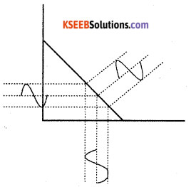
Give the graphical representation of amplification for small signal by choosing Q point near to cut off, active and saturation region.
Answer:
1. When the Q point is at the centre of the load line:
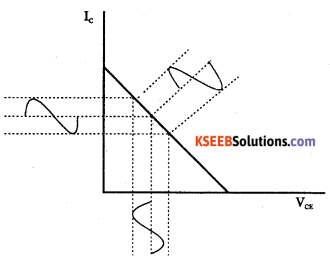
2. When Q point is near to saturation.
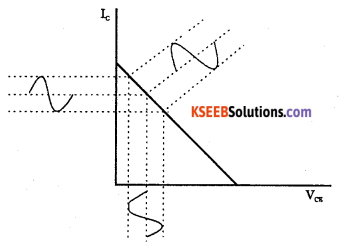
3. When Q point is nearer to cut-off.
Question 4.
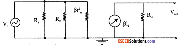
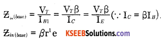
Derive the expressions for the current gain, voltage gain, input impedance, output impedance and power gain for CE amplifier with re1 model.
Answer:
AC equivalent circuit of CE amplifier using re1 model,
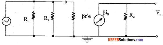
Expression for current gain:
Current gain is the ratio of output current to input current.
Current gain, = \(A_{t}=\frac{1}{i_{s}}=\beta\)
![]()
Expression for input impedance:
Input impedance is the ratio of input voltage to the input current.
\(Z_{i n}=\frac{V_{i n}}{I_{i n}}\)
This is total input impedance includes biasing resistors and impedance looking into base of the transistor.
Zin = R1 || R2 || Zin (base)
Impedance looking directly into the base is
Expression for Output impedance: Output impedance is the ratio of output voltage to output current. Output impedance \(Z_{o}=\frac{V_{o}}{i_{o}}=\frac{R_{C} i_{C}}{i_{C}}=R_{C}\)
If RL is the load resistance, then output impedance is equal to Zo = Rc || RL
Expression for voltage gain:
Voltage gain of an amplifier is the ratio of output voltage to input voltage.
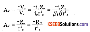
Expression for the power gain:
Power gain of an amplifier is the ratio of output power to input power.
\(\mathrm{A}_{P}=\frac{\mathrm{P}_{o}}{\mathrm{P}_{i}}\)
Power gain is also equal to the product of voltage gain and current gain.
Question 5.
Draw the circuit diagram and explain with graph the frequency response of CE amplifier.
Answer:
At low frequencies, coupling and by pass capacitors offer large reactance. As this reactance is in series with source resistance, it attenuates the input signal. As a result, gain decreases with decrease in frequency.
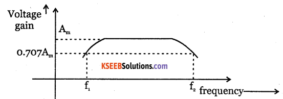
At higher frequencies, the reactance offered by junction capacitance of the transistor and wiring capacitance becomes very low. As this is in parallel with output resistance, the gain decreases with increase in frequency.
In mid-frequency range, the resistance offered by the coupling and by pass capacitors become small and negligible. Also reactance offered by junction and wiring capacitance is quite large and negligible. Hence the gain remains a constant.
Question 6.
Write a note on applications of CB, CE, CC amplifiers?
Answer:
CB amplifier: It is used to match low input impedance circuit with the high impedance load. As it is suitable for amplifying high frequencies, it is used as voltage amplifier in RF circuits. CE amplifier: It is used in applications where high voltage gain and power gain are required. Its important applications are as
- RF amplifier.
- AF amplifier.
- Signal generator.
CC amplifier: It is mainly used as buffer amplifier to match high impedance circuit with Sow impedance load for maximum power transmission. It is used as power amplifier and current amplifier.
![]()
Question 7.
Draw the circuit diagram and explain the working of CE amplier. Also mention any two applications.
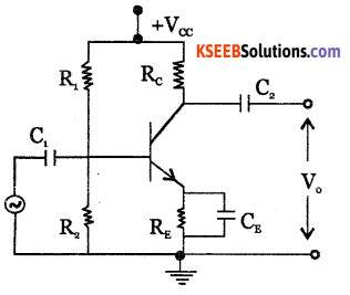
Answer:
The power supply Vcc, resistors R1, R2, Rc and RE provide required DC bias for the transistor, C1 and C2 are blocking capacitors which allow ac and block dc. The bypass capacitor CE bypass es ac at the emitter to ground.
During positive half cycle at the input signal, forward bias on the emitter base junction increases. Hence the currents ib and ic increase. As a result, ic R increases and V decreases because VCE = VCC -icRc
Thus we get negative half cycle at the output. During negative half cycle of input signal, forward bias on the emitter junction decreases. Hence ib, ic decrease and icRc also decreases. As VCB = VCC – icRc , VCE increases.
Thus, we get positive half cycle at the output.
Thus a phase shift of 180° exists between the input and the output.
Applications: It is used as AF amplifier, RF amplifier and signal generator.
Question 8.
Draw the circuit diagram and explain the working of a CB amplifier. Also mention any two applications.
Answer:
The weak signal to be amplified is applied to emitter-base junction and output signal is taken across collector-base junction.
The DC power supply, R1, R2, RE, Rc provide the required biasing for the transistor. Capacitor C1, C2 block dc and allow ac to pass through. Capacitor CB by passes ac to the ground. During positive half cycle of input signal, the forward bias between base-emitter junction decreases, as VBE is already negative with respect to the ground.
Hence iE and ic. decrease and ic Rc also decreases.
VCB =Vcc – ic Rc . As ic Rc decreases, VCBincreases. Hence we get amplified positive half cycle. During negative half cycle of the input signal, forward bias is increased because VBEis negative w.r.t. the ground.
Hence iC , iE are increased and ic Rc is increased. As VCB =Vcc – ic Rc when ic Rc increases, output voltage VCB decreases.
Thus, the positive going input signal produces positive going output signal and negative going input signal produces negative going output signal. Hence in CB amplifier, the input and output signals are in phase.
![]()
Question 9.
Draw circuit diagram and explain the working of CC amplifier. Also mention any two applications.
Answer:
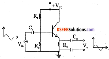
The stable operating point in the active region is obtained by R1 R2, RE. The input is applied between base and emitter and the output is taken across the emitter resistance RE During the positive half cycle of the input signal, forward bias on emitter base junction increases.
Hence iB, iE increase and output voltage iERE increases. Thus, during positive half cycle of the input, we get positive half cycle at the output. ‘
During the negative half cycle of the input signal, iB and iE decrease and hence output voltage iERE decreases. Thus output and the input are in phase and the voltage gain is 1 as input signal is equal to output signal.
CC amplifiers are used in
- Power amplifiers
- Current amplifiers
- Impedance matching devices.
![]()
Question 10.
Explain with the circuit diagram, the working of RC coupled CE amplifier. Also explain the frequency response.
Answer:
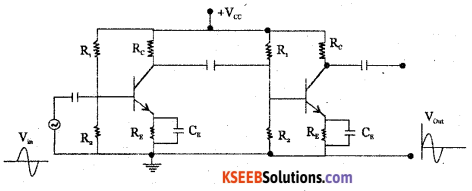
The circuit diagram shows the two stage RC Coupled transistor amplifier using voltage divider bias in CE configuration. The connection to second stage from the first stage is done through the coupling capacitor Cc.C1 couples input signal to first stage and C2 couples the signal from first stage to the second stage.
R1,R2 provide the required biasing and RE provides the stabilization. CE bypasses ac across the resistor Rc.
When the ac input signal is applied to the input of the first stage, it gets amplified and appears at its output with a phase difference of 180° This amplified signal is fed to the input of the second stage through the coupling capacitor C2. The second stage further amplifies the signal and produces a phase reversal of 180° with respect to its input signal. The signal is inverted twice and the input and output of two stage CE amplifier are in phase.
Frequency response:
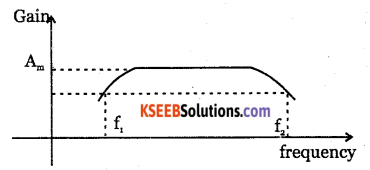
At low frequencies, the coupling capacitor Cc offers high reactance Xc. Hence it allows only a small part of the signal to pass from one stage to the next stage. Thus gain is less at low frequencies.
At high frequencies, the coupling capacitor Cc offers a low reactance and acts like a switch. Hence , due to loading effect of the next stage increases and the gain decreases.
In mid-frequency range, the effect of coupling capacitor is such that it maintains a constant voltage gain. When the frequency increases, the capacitive reactance Cc decreases which tries to increases the gain. As the capacitive reactance decreases, the loading effect of next stage reduces the gain. The voltage gain remains a constant as the two factors cancel each other.
![]()
Question 12.
With input and output waveforms, explain class-A, Class B, Class C and Class AB power amplifiers.
Answer:
The four types of power amplifiers are:
i. Class A: In class A operation of an amplifier, the Q point is located exactly at the centre of linear amplifying region of the characteristic. The current in the output circuit flows for full cycle of the input signal.
ii. Class B: In class B operation, the Q point is located at the cut off region. The output current will flow only for half the cycle of the input signal.
iii. Class AB: Q point is located between X-axis and the centre of the load line. The output current flow for more than half cycle and less than full cycle of the input signal.
iv. Class C: The Q point is located beyond the cut-off region, below the X-axis. The output current flows for less than half of input signal.
Question 13.
With a circuit diagram, explain the working of class B push pull amplifier.
Answer:
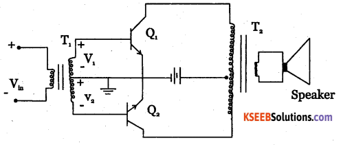
Class B push-pull amplifier is as shown in the diagram. T1 and T2 are two centre tapped transformers and Q1, Q2 are two identical transistors. Transformer T1 produces signal voltages V1 and V2 which are 180° out of phase with each other.
These two signals are applied to the Polarities reverse during negative half cycle of input voltage. Q2then is ON and Q1 is OFF. Q2amplifies the signal and the alternate half cycle appears across the loud speaker.
two transistors. Transformer T2 couples AC output signal from collector to loud speaker. The two emitters are connected to centre tap of transformer T1 secondary and Vcc to the centre tap of T2 secondary.
During positive half cycle of input voltage, secondary winding of T1 has voltages V, and V2. Transistor Q1, conducts and Q2 is cut off. The collector current through Q1 produces an amplified and inverted voltage which applied to loud speaker through a transformer.
![]()
Question 14.
Explain with the circuit diagram, the action of class C collector tuned power amplifier
Answer:
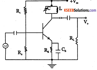
It has parallel tuned circuit as collector load. The value of capacitance and inductance of tuned collector are selected such that it resonates with the same frequency, which is equal to frequency to be amplified.
The high frequency signal to be amplified is given to the input of the amplifier. The resonant frequency of parallel tuned circuit is made equal to frequency of signal by changing value of capacitor. Then the tuned circuit offers very high impedance. If the input signal has several frequencies, amplifier will select and amplify those frequencies which are close to resonant frequency. In this way, the amplifier selects and amplifies the desired frequency.
Question 15.
Compare four types of power amplifiers.
Answer:
| Class | A | B | C | AB |
| Conduction angle |
360° | 180° | Less than 90° | 180° to 360° |
| Position of Q point | Centre of load line. | on x-axis (cut off) | Below x-axis | Between x-axis and centre of load line |
| Overall efficiency |
25% | 70-80% | Higher than 80% | 50-70% |
| Signal distortion |
None | At x-axis cross over point | Large Amounts |
Small amounts. |
Problems with Solutions
Question 1.
The microphone converts audio frequency sound into electrical signal of 5mV and is connected to a CB amplifier having input impedance of 25Ω and output impedance of 500 kQ and load resistance 5kΩ. Find the output voltage.
Answer:
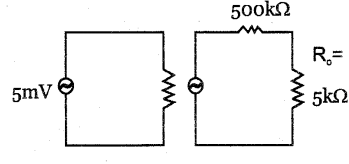
\(\mathrm{I}_{i}=\frac{\mathrm{V}_{i}}{\mathrm{Z}_{i}}=\frac{5}{25 \times 10^{3}}=0.2 \mathrm{mA}\)
V0 = I0 R0
= I0 R0 (∵ In CB amplifier, Ii = Ii)
= 0.2 x 10-3 x 5 x 103
= 1V.
![]()
Question 2.
Calculate the input impedance of CE amplifier given IE=4.5mA, β = 180 for a Si transistor.
Answer:
For Si transistor, re1
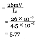
Input impedance,β re1 = 180 x 5.77
= 1038.6Q
= 1.038k£L
Question 3.
Find the bandwidth and gain at 3dB line for an amplifier having mid-band gain of 600 haveing 3 dB frequencies 100Hz and 300kHz.
Answer:
Bandwidth = f2 = f1
= 300kHz – 100
= 3,00,000 – 100
= 299900 Hz
=299.9kHz
Gain at 3dB \(=\frac{A_{m}}{\sqrt{2}}=\frac{600}{\sqrt{2}}\)
= 424.32
Question 4.
In an amplifier, maximum voltage gain is 2000 for signal frequency of 2 It falls to 1414 at 10KHz and 50Hz. Find bandwidth, lower cut off frequency and upper cut off frequency.
Answer:
Bandwidth = f2 = f1
= 10kHz – 50
= 10,000-50
= 9950Hz
= 9.95kHz.
f2 = 50Hz,
f1 = 10kHz.
Question 5.
The voltage gain of two stage amplifier is 70 If the input voltage is 5|iV, find the output voltage.
Answer:
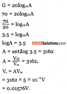
![]()
Question 6.
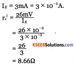
The DC emitter current of transistor is 3 Calculate the AC resistance of emitter diode of silicon transistor.
Answer:
Question 7.
A three stage amplifier has a first stage voltage gain of 100, second stage voltage gain of
Answer:
A1 = 100, A2 = 200, A3 = 400.
ATotal A1 x A2 x A3
= 100 X 200 X 400 = 8 x 10⁶
Gain in dB = 20 log Atm
= 20 log 8 x 106
= 20 x (6.9031)
= 138.02dB.
Question 8.
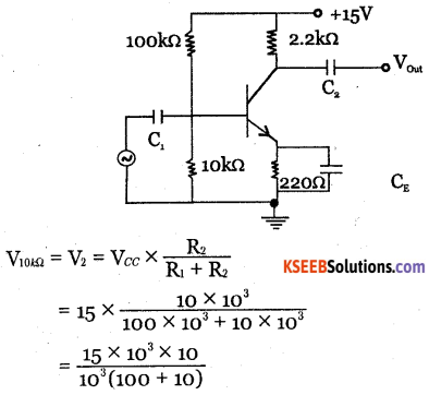
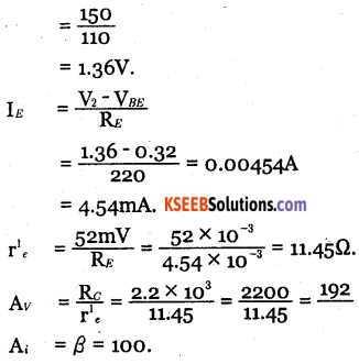
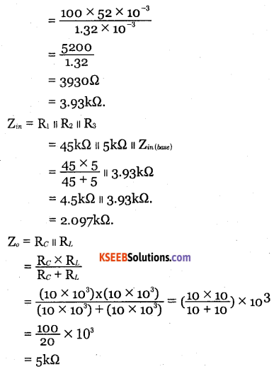
200 and third stage voltage gain of 400. Find the total voltage gain in dB. CE amplifier circuit using germaniuntransistor is as shown in the figure. Calculate
i. The voltage across 5kΩ
ii. IE
iii. Zin (base)
iv. Zin
v. Z0 Given re1 = \(\frac{52 m V}{I_{E}}\), β = 100.
Answer:
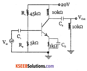
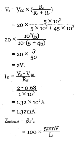
![]()
Question 9.
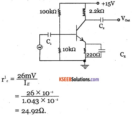
For CE amplifier circuit using silicon transistor, find
i. r’e ii. Av iii. V0 IV. A. V. Ap. VI. Gp given IE = 1.043mA and β = 100.
Answer:
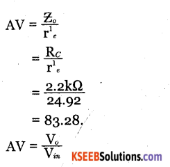
V0 = Av Vin
= 83.28 x 10 x 10-3
= o.8328Volt.
Ai= 0 = 100.
Ap = Ai Av
= 100 x 83.28 = 8328.
Gp = 10 log Ap
= 10 log 8328
= 10 x 3.9205
= 39.05dB.
Question 10.
For CE amplifier circuit using Germanium transistor, given below, find 1
i. Voltage across 10kΩ
ii. IE
iii. r3 e
IV. Av
Answer: