Students can Download 2nd PUC Electronics Chapter 9 Power Electronics and its Applications Questions and Answers, Notes Pdf, 2nd PUC Electronics Question Bank with Answers helps you to revise the complete Karnataka State Board Syllabus and score more marks in your examinations.
Karnataka 2nd PUC Electronics Question Bank Chapter 9 Power Electronics and its Applications
2nd PUC Electronics Power Electronics and its Applications One Mark Questions and Answers
Question 1.
What is power electronics?
Answer:
Power electronics is the application of solid state electronics for the control and conversion of electric power.
Question 2.
Mention one application of power devices.
Answer:
Turn on and turn off operations in power control circuits.
Question 3.
Mention any two power conducting devices.
Answer:
- Power diode.
- Power bipolar junction transistor.
Question 4.
What is a power diode?
Answer:
Power diode is the power level counters part of the low power signal diodes.
![]()
Question 5.
Which layer is also called as “drift layer” in power diode?
Answer:
“Drift layer” is lightly doped region between two heavily doped P and n layers.
Question 6.
Draw the circuit symbol of a power diode.
Answer:

Question 7.
Which is lightly doped layer in power diode?
Answer:
n epitaxial layer.
Question 8.
Which are the two heavily doped layers in power diode?
Answer:
n+ substrate.
Question 9.
What is the magnitude of impurity atom densities in drift layer?
Answer:
1014/Cm3.
Question 10.
Is the drift layer present in low power diodes?
Answer:
No.
![]()
Question 11.
What is the space charge region?
Answer:
Space charge region is the region where accumulation of electrons take place.
Question 12.
Write an expression for the voltage drop across forward conducting power diode.
Answer:
VAK = V + VRD. Where V. is the drop across P+ n– junction.
Question 13.
Give the expansion of PBJT.
Answer:
Power bipolar junction transistor.
Question 14.
Draw the circuit symbol of npn PBJT.
Answer:

Question 15.
What are the operating regions of PBJT.
Answer:
- Active region.
- Saturation region
- Cut off.
Question 16.
What is the second breakdown phenomenon?
Answer:
Second breakdown phenomenon is that where thermal runaway quickly takes place when the junction temperature beyond safe limit and the device is destroyed.
Question 17.
Expand SCR.
Answer:
Silicon controlled rectifier.
Question 18.
What is the other name for SCR?
Answer:
Thyristor.
Question 19.
How many PN junctions are there in SCR?
Answer:
Two.
![]()
Question 20.
Draw the schematic diagram of SCR.
Answer:

Question 21.
Expand LASCR.
Answer:
Light activated silicon controlled rectifier.
Question 22.
Expand RCT.
Answer:
Reverse conducting thyristor.
Question 23.
Expand GTO.
Answer:
Gate turn off Thyristor.
Question 24.
Draw the circuit symbol of thyristor.
Answer:

Question 25.
Draw the equivalent circuit of thysistor in terms of two transistors.
Answer:

Question 26.
Write an expression for SCR anode current when positive gate current is applied.
Answer:
\(I_{ A }=\frac { \propto _{ 2 }I_{ G }+I_{ C_{ 0 } } }{ 1-\left( \propto _{ 1 }+\propto _{ 2 } \right) } \)
![]()
Question 27.
What is latching current?
Answer:
Latching current is that current such that when anode current is greater than it, the thyristor will be in ON state.
Question 28.
What is holding current?
Answer:
Holding current is that current such that when anode current is less than it. the thyristor is turned OFF.
Question 29.
What is natural (line) commutation?
Answer:
In ac circuit with resistive loads, turn off happens automatically during negative zero crossing of supply voltage. This is called natural or line commutation.
![]()
Question 30.
What is forced commutation?
Answer:
Forced commutation is the arrangement made with dc circuits to ensure an OFF condition.
Question 31.
Mention an application of TRIAC.
Answer:
Residential lamp dimmers, heater control.
Question 32.
Mention any one unidirectional semiconductor controlled device.
Answer:
Power diode.
Question 33.
Mention any one bidirectional semicondutor device.
Answer:
TRIAC.
Question 34.
Draw the circuit symbol of TRIAC.
Answer:

Question 35.
Name the terminals of a TRIAC.
Answer:
- Main terminal 1(MT1)
- Main terminal 2 (MT2).
- Gate
Question 36.
Expand MOSFET.
Answer:
Metal oxide semiconductor field effect transistor.
Question 37.
Name the terminals of power MOSFET.
Answer:
- Gate
- Drain
- Source
![]()
Question 38.
Draw the circuit symbol of n-channel enhancement power MOSFET.
Answer:

Question 39.
Draw the circuit symbol of n-channel depletion power MOSFET.
Answer:

Question 40.
What is the inversion layer in power MOSFET
Answer:
The layer of free electrons at the interface between the gate oxide and the P type body.
Question 41.
Expand IGBT.
Answer:
Insulated gate bipolar transistor.
Question 42.
Draw the circuit symbol of IGBT
Answer:

Question 43.
Write the expressions for load voltage and load current of a single phase fully controlled half wave rectifier.
Answer:

Question 44.
Write the expression for firing angle of half wave rectifier with RC triggering circuit.
Answer:
\(\alpha=180-\left(\frac{x}{y / 2}\right) \times 180\)
Question 45.
Write the expression for firing angle of full wave rectifier with RC triggering circuit.
Answer:
\(\alpha=\left[\frac{x}{\mathrm{y}}\right] 180\)
Question 46.
Write the expressions for load voltage and load current of SCR full wave rectifier using RC triggering circuit.
Answer:

Question 47.
Name the device which converts AC to unipolar DC current.
Answer:
Rectifier.
Question 48.
What is the function of AC voltage controller?
Answer:
AC voltage controller is used to get AC of desired magnitude from line AC.
![]()
Question 49.
Which power semiconducting device is used in the construction of single phase AC
voltage controller?
Answer:
TRIAC.
Question 50.
What is the function of DC chopper?
Answer:
The chopper is used to convert a DC voltage of fixed amplitude to the DC of variable pulse width.
Question 51.
Draw the symbol of DC chopper.
Answer:

Question 52.
What is the function of inverter?
Answer:
Inverter converts DC to AC of desired voltage and frequency.
Question 53.
Write an expression for the average voltage of a DC chopper.
Answer:
\(\mathrm{V}_{a r g}=\left[\frac{\mathrm{T}_{O N}}{\mathrm{T}}\right] \mathrm{V}_{S}\)
Question 54.
What is the duty ratio of a chopper?
Answer:
Duty ratio = \(\frac { T_{ ON } }{ T } \)
Question 55.
Mention an application of DC to AC inverters.
Answer:
Inverters are used for variable speed AC motor drives, induction heating.
![]()
Question 56.
What are gate drive circuits?
Answer:
Gate drive circuits are circuits that control terminal characteristics to efficiently turn ON or OFF device of the convertor.
Question 57.
What are pulse transformers?
Answer:
Pulse transformers are used for electrical isolation between gate circuit and the load circuit.
Question 58.
What are opto-couplers?
Answer:
Optocouplers transfer electrical signal from one circuit to another, while electrical signal from one circuit to another, while electrically isolating two circuits from one another.
2nd PUC Electronics Power Electronics and its Applications Two Marks Questions and Answers
Question 1.
Write a note on application of power electronics.
Answer:
Control of electric current in power devices controls various power systems built with the power devices. Power electronics is based on the switching properties of power semiconductor devices.
Question 2.
Write a note on power semiconducting devices.
Answer:
The important applications of power devices are AC to DC rectifier, AC to AC Voltage controller, DC-DC chopper and DC to AC inverter. These devices are used in power products such as heat controls, light controls, motor controls, power supplies etc.
Question 3.
What are the functionalities of a power diode?
Answer:
Power diode is used as residential lamp dimmers, heater control and for speed control of motors.
![]()
Question 4.
Draw the schematic cross-section of power diode.
Answer:

Question 5.
What are the magnitudes of impurity atom densities in two heavily doped layers of power diode?
Answer:
1019/Cm3and 10’VCm3.
Question 6.
Distinguish between punch through and non-punch through type power diodes.
Answer:
In non-punch through diodes, the depletion region boundary does not reach the end of drift layer. In punch through diode, the depletion layer spans the entire drift region and is in contact with n+ cathode.
Question 7.
Draw the forward and reverse characteristics of power diode.
Answer:

Question 8.
Write the expression for the current through the power diode and explain its terminology.
Answer:
\(I=I_{ S }\left[ e^{ \frac { QV }{ kT } }-1 \right] \)
Is= reverse saturation current.
V = applied voltage across the diode.
Q = Charge of an electron.
K = Boltzmann constant = 1.381 x 10⁻²³JK-1
T= absolute temperature in kelvin.
![]()
Question 9.
How a power BJT can be constructed?
Answer:
A bipolar transistor is formed by adding a second P’ or n’ region to pn junction diode. With two n regions and one p-region, two junctions are formed and it is known as npn transistor. With two p regions and one n-region, it is called pnp transistor. The three terminals are named as collector, base and emitter. To block large voltage during OFF state, a lightly doped base p region and heavily doped collector n+ are used
Question 10.
Write a note on classification of saturation region in power transistor.
Answer:
1. Quasi-saturation region:
This region is due to introducing drift region into the structure of a power transistor. The base- collector region is forward biased and the base current still has some control over collector current.
2.Hard saturation region:
In this region, base current has no control over the collector current. The collector current depends on collector load and the biasing voltage Vcc.
Question 11.
Draw the schematic construction of SCR.
Answer:

Question 12.
What are latching current and holding current?
Answer:
Latching current is that current such that when the anode current is greater than it, the thyristor will be in ON state. Holding current is such that when anode current is less than it, the thyristor is turned off.
Question 13.
Draw VI characteristics of SGR.
Answer:

Question 14.
Write a note on construction of SCR.
Answer:
The primary crystal is of lightly doped n type on either side of which two p layers with higher doping levels are grown. Depletion layer spreads mainly into the lightly doped n’region. The outer n+ layers are formed with doping levels higher than both p type layers. The top p layer acts as the anode terminal while the bottom n layers act as cathode. The gate terminal connections are made to the bottom p layer.
![]()
Question 15.
Mention the types of power MOSFET.
Answer:
- Depletion type power MOSFET.
- Enhancement type power MOSFET.
Question 16.
Why enhancement MOSFETS are preferred more than depletion MOSFETs?
Answer:
Depletion type MOSFET are normally ON type switches ie, with gate terminal open a nonzero drain current can flow in these devices. As this is not convenient in many power electronic applications, enhancement type MOSFETS are preferred.
Question 17.
What are differences between enhancement and depletion MOSFET?
Answer:
The depletion type MOSFETS are normally ON type switches ie, with the gate terminal open a non-zero drain current can flow in these devices. As this is not convenient in many power electronic applications, enhancement type MOSFETS is mostly used in power electronics applications.
Question 18.
How is an inversion layer created in power MOSFET?
Answer:
In MOSFET, positive charge induced on the gate metallisation repels majority hole carriers from the interface region between gate oxide and p type body. Further increase in VGS makes depletion layer to increase. The immediate source oftelectron is electron-hole generation by thermal ionisation. Thus, layer of electrons at the interface called inversion layer is formed.
Question 19.
Draw the exact and approximate equivalent circuit of IGBT.
Answer:

Question 20.
Describe the operation of IGBT.
Answer:
From the input side the IGBT be haves as a MOSFET. When the gate emitter voltage is less than threshold voltage no inversion layer is formed in the p type body region and the device is in off state. The forward voltage applied between the collector and emitter drops entirely across the junction J. Under this condition, very small leakage flows through the device.
![]()
Question 21.
Why the power semiconductor devices are used in power controls?
Answer:
Power semiconductor devices are used in power controls because:
- There are no moving parts and are totally silent in operation.
- They are fast, compact and have long life.
- They are highly reliable.
- They can operate at high voltage electric mains.
Question 22.
Name the types of power converters and draw their symbols
Answer:

Question 23.
Sketch the input and output waveforms of SCR HWR.
Answer:

Question 24.
Draw the output waveforms of SCR FWR.
Answer:

Question 25.
Sketch the input and output waveform of TRIAC AC voltage controller.
Answer:

Question 26.
Sketch the output waveform of a chopper circuit for DC input of 10V and duty ratio of 75%.
Answer:

Question 27.
Sketch the output waveform of inverter circuit for DC input of 12V with a frequency of 50Hz.
Answer:

Question 28.
Write a note on gate drive circuits.
Answer:
Out of three terminals of a discrete controlled device, two are main terminals. Control terminals are one of the main terminals and the third form control terminals. The gate drive, circuits are required to turn on and turn off the devices in converters and to protect the devices. Separate isolated power supplies are required for each power device in the converter.
Question 29.
Write a note on pulse transformers.
Answer:
These are used in firing circuits for thyristors and TRIAC, for electrical isolation between gate circuit and load circuit. The isolation is required because the load may be high voltage ac supply and the load circuit uses low voltage. The transformers used have 1:1 windings.
Question 30.
Write a note on Optocouplers.
Answer:
An optocoupler or optoisolator is an electronic component that transfers an electronic component that transfers an electronic component that transfers an electrical signal from one circuit to another, while electrically isolating the two circuits from each other. It consists of an infrared light emitting LED chip that is optically in line with a light sensitive silicon semiconductor chip, all enclosed in the same package.
Question 31.
Draw the circuit diagram of opto-coupler isolator circuit for MOSFET/IGBT/Vcc
Answer:

Question 32.
What are snubber circuits?
Answer:
Snubber circuits are protection circuits which protect individual devices. Power semiconductor devices and converters must be commonly protected against over-current, over-voltage and excessive temperature rise.
![]()
Question 33.
What are advantages of static switche?
Answer:
- Static switches have no movable part and are totally silent in operation.
- They are fast, compact and have long life.
- They are highly reliable.
- They can operate with electric mains at high voltage and high current.
2nd PUC Electronics Power Electronics and its Applications Three Marks Questions and Answers
Question 1.
Why is the drift layer introduced in power diode?
Answer:
Power diodes of largest power rating are required to conduct several kilo amps of current in the forward direction with very little power loss while blocking several kilovolt in the reverse direction. Large blocking voltage requires wide depletion region. Charge density in the depletion layer should also below in order to get a wide depletion region. For these two requirements, drift layer is introduced between two heavily doped p and n layers.
Question 2.
Show that ohmic drop makes the forward V-I characteristics of a power diode more linear.
Answer:
The voltage drop across a forward conducting power diode has two components ie, VAK=VTVRD where w is voltage drop across pTv junction. The component VRD is due to ohmic drop in the drift region. VRD=RNIp where IF is forward current.
∴ Vak=Vj+RoNIf The ohmic drop makes forward V-I characteristics of a power diode more linear.
Question 3.
Explain the double injection’ mechanism in forward biased power diode.
Answer:
When p+n– junction becomes forward biased, there will be injection of excess p type carrier from p+ side into the n‘ side region. At high level of injection, excess p type carrier density distribution reaches n’ n+junction and attracts electrons from n+ cathode. This leads to electron injection into n’drift region from n+ junction. This mechanism is called ” double injection”.
![]()
Question 4.
Write a note on secondary breakdown phenomenon in PBJT.
Answer:
The maximum collector-emitter voltage that a power transistor can withstand in active region is determined by base collector avalanche breakdown voltage. This voltage Vsus can be ‘ attained for relatively lower values of collection current. At higher levels of collector currents, the allowable active region is further restricted by ” The second breakdown”.
Question 5.
Obtain the expression for the anode current of SCR when the gate current is zero.
Answer:
When gate terminal is open, IG = 0. Then J1, and J3 are forward biased and J2 is reverse biased
Then Ic1 =α1 IA + ICu1 — (1)
Ic2 =α2 IA + ICu2 — (2)
α1,α2 are current gains of transistor Q1 and Q2
while ICu1 and ICu2 are reverse saturation currents.
We have IA = Ic1+ Ic2 — (3)
Equation (3) becomes,
IA = α1 IA + ICu1 + α2 Ik + Iω2 —-(4)
It = Ia + Ic = IA
Put Ik = IA .in equation (4),
IA = α1 IA + ICu1 + α2(IA +Ic ) +ICu2
Solving this equation,
\(I_{ A }=\frac { I_{ Cu1 }+I_{ Cu2 } }{ 1-\left( \alpha _{ 1 }+\alpha _{ 2 } \right) } +\frac { I_{ CO } }{ 1-\left( \infty _{ 1 }+\infty _{ 2 } \right) } \)
Where ICuo = ICu1+ ICu2
Question 6.
Draw the schematic symbol of TRIAC and explain its terminals.
Answer:

MT1 = Main terminal 1.
MT2 = Main terminal 2.
G = Gate
Question 7.
Write a note on construction of PBJT.
Answer:
Power Bipolar junction Transistor is the first semiconductor device to allow full control over turn on and turn off operations in power control circuits. A bipolar transistor is formed by adding a second p” or n– region to pn junction diode. With two n regions and one – p region, two junctions are formed and it is known as npn transistor. The three terminals are named Emitter, Base, collector.

In order to block large voltage during OFF state a lightly doped collection drift region is introduced between the moderately doped base (p) region and heavily doped collector (n+) region. In order to maintain a large current gain p, the emitter (n+) doping density is made several orders of magnitude higher than the base (p) region. The emitter base depletion region does not penetrate considerably into the base. Hence, the width of the base region in a power transistor is more as compared to that in a signal level transistor. A power BJT has vertically oriented alternating layers of n and p type semiconductor.
The vertical structure is preferred for power transistors because it maximises the crosssectional area through which the on current flows. In this way, the resistance and power loss is minimised.
![]()
Question 8.
Explain the operation of power transistor
Or
Explain the conditions to operate power transistor under active and saturation regions. Answer:
When biasing voltages are applied, the emitter base junction becomes forward biased and collector base junction is reverse biased. Potential barrier and depletion region width reduces. As potential barrier is reduced, a large number of minority charge carriers are introduced in emitter and base regions. Few minority charge carriers reaching base recombines with majority carriers. The rest defuse to edge of depletion region where they are swept away to the collector region by the large electric field. Under this condition, the transistor is said to be in active region.
When VQE is increased, the injected minority charges into the base region increases and base – and collector currents also increases. The voltage Vcg decreases with increase in the collector current due to increasing drop in the external resistance Rc, as the collector base voltage Vcc is constant.
Hence potential barrier starts decreasing and at one point it becomes forward biased. Due to forward biasing there will be minority carrier injection into the base. Under this condition, the transistor is said to be in the saturation region.
2nd PUC Electronics Power Electronics and its Applications Five Marks Questions and Answers
Question 1.
Describe the construction of SCR.
Answer:
Silicon controlled rectifier or thyristor is a four layer, three terminal semiconductor controlled device. It can be turned on by a current signal but cannot be turned off without interrupting main current. It can block voltage in both the directions but can conduct current only in one direction.

The primary crystal is of lightly doped n’ type on either side of which two p type layers with doping levels higher by two orders of magnitude are grown. The depletion region spreads mainly into the lightly doped n‘ region. The thickness of this layer depends on required blocking voltage of the device. During the ON condition, the ON state voltage drop is less. The outer nT layers are formed with doping levels higher than both p type layers. The top p layer acts as the anode terminal while the botton n layers acts as the cathode. The Gate terminal connections are made to the bottom p layer.
Question 2.
Explain the operation of thyristor when gate terminal is open.
Answer:

Ico = Ico1 and Ico2
Where Ico1 and Ico2 are the reverse saturation currents of CB junction of Q1 and Q2 transistros. When VAK is increased upto avalanche breakdown voltage of junction J2, Ico1 increases, both α1 and α2 values increase and α1 + α2 approaches unity. Under this condition large anode current starts flowing which is controlled only by external load resistor, The voltage drop in the external resistance causes a collapse of voltage across thyristor. The CB junctions of both Q1 and Q2 become forward biased and the total voltage drop across the device becomes equal to voltage drop across the diode. The thyristor is then said to be in ON state. Soon after
turn ON, if iA is larger than a specified current called latching current, a, and a2 remain high enough to keep thyristor in ON state. The only way thyristor can be turned OFF is bringing I below a specified current called holding current IH where α1 and α2 values start decreasing. The thyristor can region the forward blocking capacity once excess stored charge at J2 is removed by the application of a reverse voltage across A and K.
![]()
Question 3.
Explain the operation of the thyristor when positive gate current is applied,
Answer:
The thyristor can be turned ON by the application of positive current flowing from gate to cathode without increasing the forward voltage across the device upto forward break over level.
With positive gate current,
\(I_{ A }=\frac { \propto _{ 2 }I_{ G }+I_{ CO } }{ 1-\left( \propto _{ 1 }+\propto _{ 2 } \right) } \)
With sufficiently large IG, the thyristor can be turned ON for any value of I and hence VAK. This is called gate assisted turn on of a Thyristor. A thyristor is usually turned ON by this usual method only.
Question 4.
Explain the operation of SCR when it is applied with the negative gate voltage.
Answer:
When a reverse voltage is applied across a thyristor, junctions J1 and J3 are reverse biased while J2 is forward biased. Junction J3 has very low breakdown voltage as both n+ and p regions on either side of this junction are heavily doped. The applied reverse voltage is entirely supported by junction Jr The maximum value of reverse voltage is restricted by i. maximum field strength at junction J and ii. Punch through of the lightly doped n’ region.
As the P layers on either side of n_ region have almost equal doping levels, the avalanche breakdown voltages of J1 and J2 are the same. Hence forward and reverse breakdown voltages of a thyristor are almost equal. Upto the breakdown voltage of J,, the reverse current of thyristor remains constant and increases sharply after this voltage. The reverse characteristics of a thyristor are similar to that of a single diode.
Question 5.
Describe steady static V-I characteristics of SCR.
Answer:

When gate current I = 0, VAK has to increase upto forward breakover voltage VBRF before anode current starts flowing. At VBRF, the voltage across the thyristor drops to holding voltage VH, while anode current is determined by the external load. After turn ON, the thyristor is no more affected by the gate current. Any current pulse which is longer than minimum needed for TURN ON is sufficient to effect control.
Once thyristor is ON, the only way to turn it OFF is by bringing thyristor current below holding current IH. The gate terminal has no control over the turn OFF process. In ac circuits with resistive load, this happens during the negative zero crossing of the supply voltage. This is called natural commutation or line commutation. In dc circuits, some arrangement has to be made to ensure this condition and this process is called forced commutation.
![]()
Question 6.
Write a note on operation of TRIAC.
Answer:
A triac can conduct in both the directions. The conduction of a triac is initiated by injecting a current pulse into the gate terminal. The gate loses control over the conduction once TRIAC is turned ON. The TRIAC turns OFF only when the current through the main terminals becomes zero.

The three terminals of TRIAC are marked MT, (Main terminal 1), MT2 (Main terminal 2) and the gate G. As TRIAC is a bidirectional device and can have its terminals at various combinations of positive and negative voltages, there are four possible electrons potential combinations, as given below: •
- MT2 positive with respect to MT1, G positive with respect to MT1.
- MT2 positive with respect to MT1, G negative with respect to MT1.
- MT2 negative with respect to MT1, G negative with respect to MT1.
- MT2 negative with respect to MT1, G positive with respect to MT1.
In trigger mode-1, the gate current IG, flows mainly through P2N2 junction like an ordinary thyristor. When the gate current has injected sufficient charge into P2 layer, the TRIAC starts conducting through the P1, N1, P2, N2, layers like an ordinary thyristor.
In trigger mode-3, the gate current IG forward biases the P2 P3 junction and large number of electrons are introduced in the P2 region by Nr Finally the structure P2 N1, P1, N4 turns on completely.
Question 7.
Describe the steady state VI characteristics of TRIAC.
Answer:
ATRAIC is similar to two thyristors connected in anti-parallel. With no signal to the gate, the TRIAC will block both half cycles of applied ac voltage provided its peak value is lower than break over voltage (V) of the device. The turning ON of the TRIAC can be controlled by applying the gate trigger pulse at the desired instance.
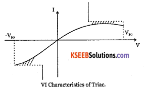
Mode-1 triggering is used in the first quadrant and Mode-3 triggering is used in 3rd quadrant. Most of the thyristor characteristics apply to the TRAIC. In a TRIAC, the two conducting paths from MT, to MT2 or from MT2 to MT1, interact with each other in the structure of the TRAIC. Voltage, current and frequency ratings of triacs are lower than thyristors. The Voltage and current rating are 1200V and 300A
Question 8.
Explain the constructional feature of power MOSFET
Answer:
The diagram shows schematic representation of a single MOSFET cell structure. A large number of such cells are connected in parallel to form a complete device. The two n+ end layers ” source ” and ” drain ” are heavily doped to the same level. The p type middle layer is termed the body and has moderate doping level.

The n’ drain drift region has the lowest doping density. The break down voltage of the device is decided by the thickness of this region. The gate terminal is placed over the n‘ and p regions of cell structure and is insulated from the semi-conductor body by a thin layer of silicon or gate oxide. The device is constructed of many thousands of small cells. The source region of all the cells on a wafer are connected to the same metallic contacts to form the source, drain region of all cells on a wafer are connected to same metallic contacts to form drain. Similarly all the gate terminals are also connected together.
![]()
Question 9.
Describe the operating principle of a power MOSFET.
Answer:
Application of positive voltage at the gate terminal with respect to source will convert the silicon surface beneath the gate oxide to an n type layer or channel connecting source to the Drain. The gate region of MOSFET, the gate oxide layer and p body silicon form a high quality capacitor. When a small voltage is applied to this capacitor structure with gate terminal positive with respect to source, a depletion region is formed in p type silicon.

The positive charge induced on the gate metallization repels majority hole carriers from the interface region between the gate oxide and p type body.
Further increase in VGS causes the depletion region to grow in thickness. The immediate source of electron is eletron-hole generation by thermal ionisation. The holes are repelled into the semiconductor bulk ahead of depletion region. As VGS increases, further density of free electrons at the interface becomes equal to the free hole density in the bulk of the body region beyond the depletion layer.
The layer of free electrons at the interface is called inversion layer. The inversion layer has all the properties of an n type semiconductor and is a conductive path or channel between the drain and source which permits flow of current between drain and source.
Since current conduction in this device takes place through an n type channel created by electric field due to gate source voltage, it is called enhancement type n-channel FET. The value of VGS at which inversion layer is formed is called ” Gate-source threshold voltage VGS ”
Question 10.
Describe the VI characteristics of a power MOSFET.
Answer:
MOSFET is a three terminal device where voltage on the gate terminal controls flow of current between output terminals, source and drain. The source terminal is common between input and output of a MOSFET. The output characteristics is a plot of drain current as a function of drain-source voltage VDS. With gate-source voltage VDS below the threshold voltage MOSFET operates in the cut off mode. No drain current flows. The maximum applied voltage should be below avalanche break down voltage of this junction to avoid destruction of the device. When VGS is increased beyond VQS (th), drain current starts flowing. For small values of VDS, ID is proportional to VDS and this mode of operation is called Ohmic mode of operation.

In power electronic applications, a MOSFET is operated either in the cut off or ohmic mode. The slope of VDS-ID characteristics in this mode is called ON state resistance rDS of MOSFET. Due to reduction of the channel resistance at higher values of VGS, rDS reduces with increase in VGS. At higher values of VDS, ID tends to saturate with increase in VDS and this is called active region.
![]()
Question 11.
Explain the construction and working of IGBT.
Answer:
The good characteristics of MOSFET and B JT technologies are integrated into Insulated Gate Bipolar Transistor (IGBT). The p+ injecting layer forms a pn junction with the drain layer and injects minority carriers into it.
The n type drain layer may have two different doping levels. The lightly doped n region is called drain drift region. Doping level and width of this layer sets the forward blocking voltage of the device. A large number of basic cells are grown on a single silicon wafer and connected in parallel to form a complete IGBJ device.

When gate-emitter voltage is less than threshold voltage, no inversion layer is formed and the device is in OFF state. When gate-emitter voltage exceeds the threshold, an inversion layer fonns in the p type body region under the gate. This inversion layer shorts the emitter and drain drift layer and an electron current flows from the emitter through this channel to the drift region.
This causes hole injection from pT collector to drain drift region. Few holes recombine with the electrons arriving at the drain drift region through the channel. The rest of the holes cross drift region to reach p type body where they are collected by the source metallization.
Question 12.
Draw the steady-state characteristics of IGBT and explain.
Answer:

V-I Output characteristics of an n channel IGBT is similar to BJT except that here controlling parameter is gate-emitter voltage.
When the gate emitter voltage is below threshold voltage, only a very small leakage current flows through the diode. The device under this condition is said to be operating in the cut off region.
As the gate emitter voltage increases beyond threshold voltage, IGBT enters into the active region of operation. The ratio of Ic and VGE is called forward transconductance of the device. As the gate enutter voltage is increased further, Ir also increases and VCE decreases. At one point, VCE becomes less than VQE – VGE (th). Under this condition IGBT enters into ohmic region and drives output pnp transistor to saturation. Then the device is said to be in saturation mode. In saturation mode, the voltage drop across IGBT remains constant reducing only slightly with increasing VGE.
![]()
Question 13.
Explain the construction and working of single phase SCR half wave rectifier with resistive load.
Answer:

At ωt=o, the input supply voltage becomes positive, thyristor T1, becomes forward biased. It turns ON when gate pulse Ig is applied at ωt = α, where a is called firing angle or delay angle. The angle after input voltage starts positive until the thyristor is first fired is called delay angle.
During the period 0 < ωt < α, the thyristor blocks the supply voltage and the load voltage remains zero. Hence no current flows during this interval, soon after gate pulse Ig is applied to the thyristor at ωt = α it turns ON. The voltage across thyristor reduces to zero and full supply voltage appears across the load. From this point onwards, the load voltage follows supply voltage.

Question 14.
Explain the construction and working of single phase SCR half wave rectifier with RC triggering circuit.
Answer:

The load is connected before RC circuit. In this circuit the capacitor voltage reduces, when SCR is conducting. Diode D2 along with D1 is used to prevent negative voltage to the gate w. r. t. the cathode. The firing angle for half wave rectifier is
\(\alpha=180-\left(\frac{x}{\frac{y}{2}}\right) \times 180\)
Question 15.
Explain the construction and working of a single phase SCR full wave rectifier with RC
triggering circuit.
Answer:

The SCR is connected with a diode bridge rectifier. The rectifier circuit converts AC to a unidirectional current through the thyristor. The voltage on the capacitor follows the diode rectifier waveform because RC circuit is connected to diode rectifier. During each half cycle when the voltage across the capacitor reaches trigger level which is just enough to supply gate trigger current to thyristor, then thyristor starts conducting. Firing angle \(\alpha=\left(\frac{x}{\mathrm{y}}\right)_{180}\)

Question 16.
Explain the working of single phase full wave AC voltage controller with resistive load.
Answer:

TRIAC is a bi-directional solid state device and conducts in both halves of ac supply. During positive half cycle MT2 becomes positive wrt MT, and gate becomes positive wrt MTr TRIAC conducts when gate pulse is injected at a firing angle a. The current follows TRIAC in the voltage wave shape from angle α to π At π, the zero crossing of the supply voltage, the TRIAC is switched OFF due to line commutation.
![]()
Question 17.
Explain the working of light dimmer circuit using a TRIAC.
Answer:

The circuit gives light illumination control using TRIAC based circuit. The TRIAC is triggered by the 32V DIAC. DIAC is a pnpn device with no gate terminal. The DIAC starts conducting in either direction if the applied voltage is more than the breakdown voltage VBR, VBR for DIAC in both the directions. One of the switching devices that can trigger a TRIAC and SCR is the DIAC.
Question 18.
Explain the working of DC to DC chopper circuit.
Answer:

The chopper is used to convert a DC voltage of fixed amplitude DC of variable pulse width. The output voltage is controlled by controlling the duty cycle of the chopper. There are used in DC power supplies, battery chargers, DC motor control.
The chopper converts fixed DC to variable DC voltage with the help of a semiconductor device. In the circuit given, the chopper is MOSFET with terminals drain D, source S and gate G. The MOSFET is connected between the source and the load. When the static device is switched ON or closed by applying proper gate pulse, the supply voltage is connected to the load.
When static device is switched OFF or opened by removing the gate signal, the load is disconnected from the supply.
The average output voltage \({ V }_{ arg }=\left[ \frac { { T }_{ ON } }{ { T } } \right] { V }_{ s }\). Where Vs is input voltage T0N is the ON time duration of the chopper.
Question 19.
Explain the working of DC to AC inverter circuit.
Answer:
Inverters convert DC power to AC power at desired output voltage and frequency. Inverters are used for variable speed AC motor drives, induction heating, aircraft power supplies, UPS for computer.

The diagram of IGBT based single phase inverter is as shown. It consists of four IGBT. The current can be supplied to the load by proper gating the IGBTs. Only two diagonally opposite IGBTs will be ON at any one time.
When Q1 and Q4 are conducting, load current flows from X to Y in the path XQ1, ABQ4 Y and load voltage is +Edc. When Q2 and Q3 are conducting, load current flows from X to Y in the path XQ3 BAQ2 Y. Now, the load current direction changes and load voltage becomes -Edc Thus, AC square wave is generated.
Question 20.
Describe the operation of opto coupler isolator circuit for MOSFET / IGBT.
Answer:

An optocoupler or opto-isolator is an electronic circuit that transfers electrical signal or voltage from one circuit to another, while electrically isolating the two circuits from each other. It has an infrared light emitting LED chip that is optically in line with a light sensitive semi conductor chip, all enclosed in the same package.
The silicon chip may be in the form of a photo diode photo transistor, or photo SCR. The two are separated by a transparent barrier which blocks electrical current flow between the two, but allows light to pass through.
Optocouplers with stand voltages between 500V and 7500V between input and output. Opto-couplers are digital switching devices for transferring either on-off control signals or digital data.
In this circuit, the gate signal generated from control unit like microcontroller is coupled to gate and source / emitter of MOSFET / IGBT. The gate signal from the control circuit is – applied to LED. When gate signal from control circuit is high, diode conducts and allows the light to fall on the phototransistor. The phototransistor then conducts and the output becomes . low. Low gate signal from the control circuit cuts off light on the phototransistor. Then the transistor does not conduct and the output becomes high.
![]()
Question 21.
Write a note on the protection of power devices and converters.
Answer:
Transients associated with switching-circuits and the faults that occur at load point stress converters and devices. Hence, serveral protection schemes must incorporated in a converter. Power semiconductor devices and converters must be protected against:
- Over-current
- \(\frac{\mathrm{d}_{i}}{\mathrm{d}_{T}}\)
- Over-voltage
- \(\frac{\mathrm{d}_{V}}{\mathrm{d}_{T}}\)
- Gate over current
- Over voltage at gate
- Excessive temperature rise.
(a) A semiconductor fuse and circuit breakers in series protect the devices against over current.
(b) Inductor in series protects against large rate of change of current.
(c) Metal oxide Varistors and crow bar circuits are used across the input supply to protect them.
(d) RC circuits called snubber circuits are used to control rate of change of voltage.
(e) Gate over current is protected by a series resistance and gate over voltage is protected by a zerer diode.
(f) Heat sink protects against excessive heat.
Problems with Solutions
Question 1.
A pn junction diode has a reverse saturation current of 100nA at 50°C. What should be value of the forward current for a voltage drop of 0.6V?
Answer:

Question 2.
Determine cathode current Ik of SCR when IG = 0. Given α1+ α2 =0.99 and
IC01,+IC02 =3mA
Answer:

Question 3.
Determine the anode current IA of SCR when gate current Ic=50mA, α1=0.495, α2=0.495 and IC01=1mA, IC02=1mA.
Answer:

![]()
Question 4.
Determine Vdc and Idc of SCR HWR. Given firing angle is 30° and rms voltage of AC input to the rectifier is 30V and the load is 10Ω.
Answer:

Question 5.
Determine Vdc and Idc of SCR HWR. Given firing angle is 0° and rms voltage of AC input to rectifier is 12V and a rheostat load of 12Q is connected.
Answer:

Question 6.
Determine average value of DC from the chopper. Given T= 2ms, TON= 0.5ms and supply voltage is 24V.
Answer:
