Students can Download 2nd PUC Electronics Previous Year Question Paper June 2017, Karnataka 2nd PUC Electronics Question Bank with Answers helps you to revise the complete Karnataka State Board Syllabus and score more marks in your examinations.
Karnataka 2nd PUC Electronics Previous Year Question Paper June 2017
2nd PUC Electronics Previous Year Question Paper June 2017
Time : 3 hrs. 15 min.
Max Marks: 70
Instructions:
- The question has five Parts A, B, C and D.
- Part – A has no choice
- Part – D has two parts. Part -1 is from problems, Part – II is of essay type questions.
- Circuit diagram/timing diagram/truth tables are drawn wherever necessary.
- Problems without necessary formula/formulae carry no marks.
Part – A
Answer all questions: 10 x 1 = 10
Question 1.
What is amplification factor?
Answer:
It is the ratio of change in drain to source voltage VDS to corresponding change in gate to source voltage VGS for constant drain current ID.
Question 2.
Define CMRR.
Answer:
CMRR is defined as the ratio of differential mode .gain to common mode gain.
Question 3.
Mention the speed of electromagnetic waves in free space.
Answer:
3 x 10⁸ ms-8
Question 4.
Mention the value of IF for AM reception.
Answer:
455 KHz
![]()
Question 5.
An FM signal has a freuency deviation of 12 KHz and modulating frequency of 6KHz. Calculate the modulation index.
Answer:
Δ= 12KHz fm = 6KHz mf = ?
\(\mathrm{m}_{t}=\frac{\Delta \mathrm{f}}{\mathrm{f}_{\mathrm{m}}}=\frac{12 \mathrm{KHz}}{6 \mathrm{KHz}}\)
Question 6.
Name the lightly doped layer in the power diode.
Answer:
Drift layer or epitaxial layer.
Question 7.
What is an octet?
Answer:
An octet is a group of eight adjacent is either in two horizontal rows or in two vertical columns.
Question 8.
Write excess-3 code for (69)10.
Answer:
| Decimal | 6 | 9 |
| BCD | 0110 | 1001 |
| Add0011 | 0011 | 0011 |
| Excess 3 code | 1001 | 1100 |
Question 9.
Why 8051 microcontroller is known as 8 bit processor?
Answer:
8051 microcontroller is called 8 bit processor because it processes 8 bits of data.
Question 10.
What is the size of an integer in C-programming?
Answer:
2 bytes.
Part – B
Answer any five questions. 5 x 2 = 10
Question 11.
Write the steps involved in drawing DC equivalent circuit of a CE amplifier.
Answer:
- Reduce all the AC sources to zero.
- Open all the capacitors.
Question 12.
A amplifier of gain 500 reduces to 100 after feedback. Calculate the feedback factor.
Answer:
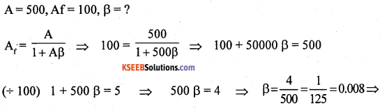
Question 13.
Distinguish between sinusoidal and non-sinusoidal oscillator.
Answer:
- Sinusoidal oscillator: Oscillator output is a sinusoidal waveform
- Non-sinusoidal oscillator: Oscillator output is a non-sinusoidal waveform.
![]()
Question 14.
Mention any two applications of power devices.
Answer:
- AC to DC rectifier.
- AC to AC voltage controller.
- DC to DC chopper
- DC to AC inverter.
Question 15.
A silicon power diode has Vj of 0.4V, R0N in drift region of 0.0020 and Ir = 75A
Answer:

Question 16.
Briefly explain the function of accumulator and program counter in microcontroller 8051.
Answer:
- Accumulator : It stores a number and on receipt of another number, adds the two and stores the sum. It can also sense the signal, clear and complement etc.
- Program counter: It holds the address of a byte in memory. It also specifies the address at the next instruction to be fetched and executed.
Question 17.
Write the meanings of the following operators in C programming,
(i) = = (ii) &&
Answer:
(i) Equal to
(ii) LoginalAND
Question 18.
Mention any two applications of RADAR.
Answer:
- Used as altimeters to measure height
- Used in defence weapons system
- Used in landing of planes in bad weather conditions.
Part – C
Answer any five questions.
Question 19.
Explain the construction of n-channel JFET.
Answer:
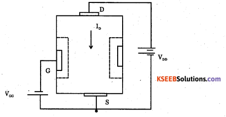
Consider n channel JFET with gate to source voltage VGG and drain to source voltage VGG. When VGG is zero, drain current is maximum and flows from drain to source called as Lcc. When V0G is increased, reverse bias across junction increases and width of depletion region across the junctions increases. Due to this channel width decreases and hence the drain current decreases. Thus the reverse voltage applied across gate to source terminal controls the drain current. When the gate to source voltage is further increased, a stage will be reached at which two depletion regions touch each other and the drain current becomes zero. Pinch off voltage is the gate voltage at which drain current becomes zero.
Question 20.
Explain the terms thermal runaway, leakage current and heat sink.
Answer:
The self destruction of an unbiased transistor due to increase in temperature and hense increase in leakage current.
Heat sink is a device which absorbs unwanted heat generated in the transistor and radiates to the surroundings. A copper conductor with different shapes are connected to the device to take out heat from the device. With heat sink, power rating of the device increases.
Leakage current is current through a device due to the motion of minority charge carriers under reverse bias conditions.
Different leakage currents are:
- Collector to base leakage current with emitter open (ICB0).
- Collector to emitter leakage current with base open (1CE0).
Question 21.
Derive an expression for input impedance of negative feedback amplifier.
Answer:
An amplifier should have high input impedance so that it will not load the preceding stage or input voltage source. High input impedance for an amplifier can be achieved with Voltage series negative feedback.
Let Ii and Vi be input current and input voltage to the basic amplifier. Vs is input to feedback amplifier, Vf is feedback voltage and vo is the output voltage.
Input impedance of basic amplifier is
\(z_{i}=\frac{V_{i}}{I_{i}}-(1)\)
Input impedance of feedback amplifier is
\(z_{v}=\frac{V_{s}}{I_{i}} \rightarrow(2)\)
Input voltage to basic amplifier with negative feedback is
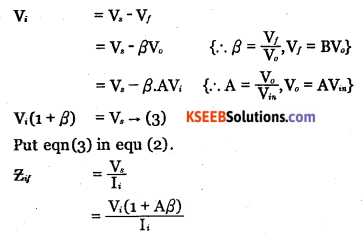
\(=\left(\frac{V_{i}}{I_{i}}\right)(1+A \beta)\)
Zif = Zi (1+Aβ)from eq ………… (1)
As (1 + Aβ) > 1 for negative feedback, Zif > Zi
Hence with negative feedback, input impedance of an amplifier increases.
![]()
Question 22.
Define critical angel, critical frequency and skip distance
Answer:
Skip distance is the minimum distance measured between transmitting antenna and the first receiving antenna measured along the surface of the earth after propagation through the ionosphere.
Critical angle for a given layer is the maximum angle of incidence of a radio wave under ionospheric propagation that gets returned to the earth.
Critical frequency for a given layer is the highest frequency of a beamed radio wave that will be returned to the earth.
Question 23.
What is demodulation? Draw the circuit diagram of linear diode detector.
Answer:
Demodulation is the process of recovering a modulating signal from the modulated wave.
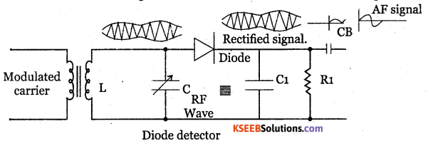
LC tank circuit is used as a parallel resonant circuit. The resonant frequency of the circuit can be varied by varying the value of capacitance C and hence RF signal of any desired frequency can be tuned in.
When a selected modulated signal is applied to the diode, the diode conducts only during the positive half of the modulated wave. Thus the diode removes the entire negative half cycles. Across R1C1 only positive half cycles of carrier modulated wave appears. Thus the low pass filter made up of R1 C1 removes the RF.
During positive half cycle, diode conducts the capacitor C1 gets charged. During negative half cycle of the carrier and diode doesnot conduct but C1 discharges through R1. Hence output is obtained. The spikes can be reduced by proper choice of R1 C1 and depth of modulation. The capacitor CB removes Dc component produced by the detector.
Question 24.
Explain non-punch through type power diode.
Answer:
In non-punch through diodes, the depletion region boundary does not reach the end of drift layer. In punch through diode, the depletion layer spans the entire drift region and is in contact with n+ cathode.
Question 25.
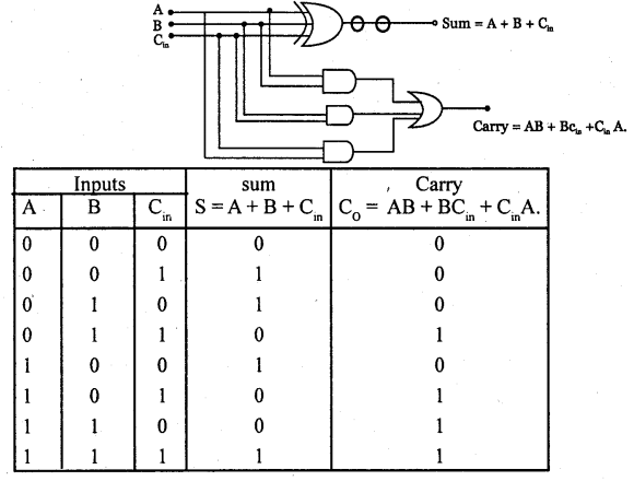
Draw the logic circuit of a full-adder using 3 input XOR gate. Write the Boolean expression for outputs SUM and CARRY.
Answer:
Full adder is a combinational logic circuit that performs arithmetic sum of three bits and gives their sum and carry .
Question 26.
List the additional features of 3G and 4G cell-phone systems.
Answer:
Additional features of 3G and 4G phone systems are:
- Colour LCD screens
- Digital cameras
- E-mail, Games
- GPS, Bluetooth
- Internet access
- Video conferencing
Part – D
Answer any Five questions. 3 x 5 = 16
Question 27.
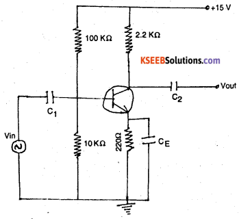
For CE amplifier circuit using Germanium transistor given below. Find
i) Voltage across 10KQ
ii) IE
iii) re
iv) Av [Given VBE = 0.32V]
Answer:
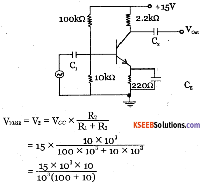
![]()
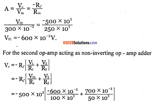
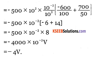
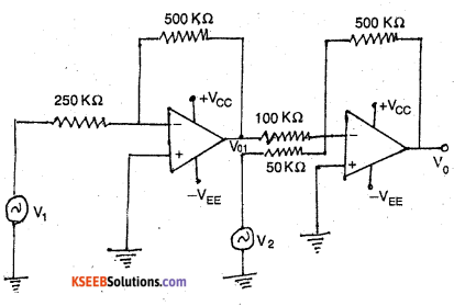
Question 28.
Calculate output voltage if V1 = 300mV and V2 = 700mV.
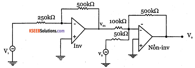
Answer:
Question 29.
A colpitts oscillator oscillates at 1.13MHz. If inductor in the feedback network has a value of 20μH and one of the capacitor value is 0.1 μF. Calculate the value of the other capacitor.
Answer:
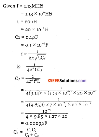
![]()
Question 30.
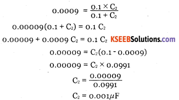
A sinusoidal carries voltage Vc = 80 sin 2π x 105 t is amplitude modulated by a sinusoidal voltage
Vm = 32 sin 2π x 103t . Write the equation of the AM wave and draw its output frequency spectrum.
Answer:
Question 31.
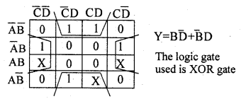
Simplify the given equation using K-map. Y = Σm (1, 3, 4, 6, 9) + Σd (11,12,14) and identify the logic gate for the simplified output expression.
Answer:
Part – E
Answer any Four questions.
Question 32.
What is direct-coupled amplifier? With neat circuit diagram explain the working of direct-coupled amplifier and draw the frequency response curve.
Answer:
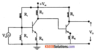
The direct coupled amplifier using two npn transistors is as shown in the diagram. In this method, output of first stage is directly coupled to the input of second stage. Resistors R1 and R2 form voltage divider circuit. Any signal at the base of the first transistor is amplified A, times and appears at the collector of first stage.
![]()
It is then applied to the base of transistor in the second stage. Hence it is amplified A2 times. The gain of the direct coupled amplifier is A = A x A. Direct-coupled amplifiers are used to amplify extremely low frequency signals.
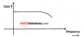
Frequency Response of Direct coupled transistor amplifier.
Question 33.
What is op-amp subtractor? Derive an expression for the output of op-amp subtractor with a circuit diagram.
Answer:
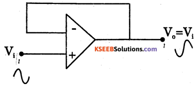
Voltage follower is Obtained by shorting Rf. The output is directly fed to inverting input terminal. Output voltage V of non-inverting
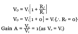
It is used as buffer amplifier for impedance matching.
Question 34.
With a neat block diagram explain the working of FM transmitter.
Answer:
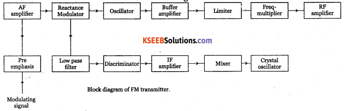
The modulating signal is applied to the pre-emphasis circuit, which improves signal to noise ratio, AF amplifier amplifies output of pre-emphasis. The processed signal is fed to reactance modulator. The reactance modulator uses a transistor or FET connected across tank circuit of carrier oscillator.
The oscillator frequency depends on the tank reactance which in turn depends on the instantaneous amplitude of modulating signal. Thus, output of reactance modulator will be a frequency modulated wave.
The oscillator is followed by a buffer amplifier which isolates oscillator from subsequent stages. The limiter maintains the amplitude constant. Class C power amplifier amplifies modulated wave to required power levels. The FM signal is then fed to the transmitting antenna.
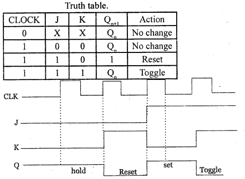
Question 35.
Explain the working of JK flip-flop with logic circuit and truth-table. Draw its timing diagram.
Answer:
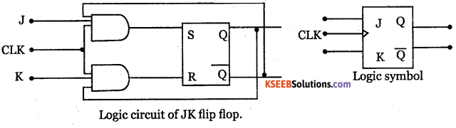
- When J = 0, K= 0, the S and R inputs are both at 0 and hence the output is in the HOLD state.
- When J = 0, K = 1, S input is at 0 while R can be either at 0 or 1, but output is always in the RESET state.
- When J = 1, K = 0, S input can be 0 or 1 but R input is always at logic 0 and hence the output remains at a stable SET state.
- When J = 1, K = 1 the Flip flop goes to complementary’ state of previous output i.e, flip flop toggles
![]()
Question 36.
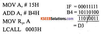
Write an assembly language program to add two numbers 1FH and B4H and store the result in R7. Verify the result by binary addition.
Answer:
Question 37.
What is debugging? Explain the different types of error that occur in C programming language?
Answer:
The process of detecting and correcting errors in the program is debugging.
C is a powerful, flexible, portable and structured programming language.