Students can Download 2nd PUC Electronics Previous Year Question Paper March 2017, Karnataka 2nd PUC Electronics Question Bank with Answers helps you to revise the complete Karnataka State Board Syllabus and score more marks in your examinations.
Karnataka 2nd PUC Electronics Previous Year Question Paper March 2017
2nd PUC Electronics Previous Year Question Paper March 2017
Time : 3 hrs. 15 min.
Max Marks: 70
Instructions:
- The question has five Parts A, B, C and D.
- Part – A has no choice
- Part – D has two parts. Part -1 is from problems, Part – II is of essay type questions.
- Circuit diagram/timing diagram/truth tables are drawn wherever necessary.
- Problems without necessary formula/formulae carry no marks.
Part – A
Answer all questions: 10 x 1 = 10
Question 1.
Write the function of source in JFET.
Answer:
Source supplies charge carriers for current conduction.
Question 2.
Name the power amplifier in which conduction angle is 360°.
Answer:
Class A.
Question 3.
Define slew rate.
Answer:
Slew rate is the rate of change of output.
Question 4.
What is the frequency of modulating signal if the bandwidth of AM wave is 10 KHz?
Answer:
\(f_{\mathrm{m}}=\frac{\mathrm{BW}}{2}=\frac{10 \mathrm{KHz}}{2}=5 \mathrm{KHz}\)
![]()
Question 5.
Define demodulation.
Answer:
Demodulation is the process of recovering original modulating signal from the modulated wave.
Question 6.
Draw the circuit symbol of IGBT.
Answer:

Question 7.
What is a counter?
Answer:
Counter is a logic circuit for counting the pulses.
Question 8.
Convert (1101)2 into gray code.
Answer:
(1011)G
Question 9.
How many interrupt sources are there in 8051 microcontroller?
Answer:
6 including RESET or 5 excluding RESET.
Question 10.
Write C equivalent expression for the mathematical expression \(\sqrt{a^{2}+b^{2}}\)
Answer:
sqrt (a*a+ b*b)
Part – B
Answer any five questions.
Question 11.
Write any two differences between FET and BJT.
Answer:
| S.No. | BJT | JFET |
| 1. | It is a bipolar device. | It is a unipolar device. |
| 2. | It is a current controlled device. | It is a voltage controlled device. |
| 3. | Current conduction is by both holes and electrons. | Current conduction is by holes or electrons. |
| 4. | Input resistance is low. | Input resistance is very high. (MCI) |
| 5. | BJT is more noisy. | JFET is less noisy. |
| 6. | Switching speed is less. | Switching speed is high. |
| 7. | Fabrication in IC is difficult. | Fabrication in IC is simpler. |
![]()
Question 12.
Mention the steps involved to obtain DC equivalent circuit of an amplifier.
Answer:
- Reduce all the AC source to zero.
- open all the capacitors.
Question 13.
Distinguish between positive feedback and negative feedback.
Answer:
- Positive feedback is the process of applying a portion of output in phase with the input.
- Negative feedback is the process of applying a portion of output out of phase with the input.
Question 14.
Write any two advantages of RC oscillators over LC oscillators.
Answer:
- RC oscillators provide constant output and good stability.
- RC oscillators do not require any inductor and hence size and cost get reduced.
Question 15.
Write Shockley’s diode equation for current through the power diode and explain its terminology.
Answer:
\(I=I_{ s }\left( e^{ \frac { qv }{ KT } }-1 \right)\)
- Is = Reverse saturation current
- T = Absolute temperature
- K = Boltzmann constant
- q = charge of electron
- V = voltage across diode.
Question 16.
Determine average value of DC from chopper. Given T= 2 ms, TQN= 0.5 ms and supply voltage is 24V.
Answer:
Duty ratio = \( \frac{T_{o N}}{T}=\frac{0.5}{2}=0.25\)
Vdc = Duty ratio x Vs = 0.25 x 24 = 6V.
Question 17.
Realise NOT and OR-gate using NOR-gate
Answer:

Question 18.
Distinguish between uplink and downlink signals
Answer:
| Uplink | Downlink |
| 1) Signal transmitted from ground station to satellite 2) Frequency range is 6 GHz |
1) Signal transmitted from satellite to ground station. 2) Frequency range is 4 GHz. |
Part – C
Answer any five questions. 5 x 3 = 15
Question 19.
What is a DC load line? Mention any two advantages of voltage divider bias.
Answer:
Operating point is the zero signal values of collector Ic and collector to emitter voltage VCE of a transistor. DC load line is a straight line drawn on the output characteristics representing output DC voltage and corresponding direct current under no signal conditions.
![]()
The operating point does not depend upon the value of β of the transistor. Hence the operating point does not change its position due to rise in temperature or replacing a transistor of different p value. Hence voltage divider bias provides excellent stabilisation and is preferred to other biasing methods.
Question 20.
Calculate the input impedance of a negative feedback amplifier if input impedance without feedback is 10 KQ. Given A = 100 and β = 0.01.
Answer:
Zif = Zi(1 +Aβ)
= 10 x 103 (1 + 100 x 0.01)
= 20 x 103 Ω
= 20kΩ
Question 21.
With block diagram, explain basic communication system.
Answer:

Question 22.
Draw the equivalent circuit of transmission lines for low frequency. Mention any two types of antennas.
Answer:

Types of Antenna:
- Helical antenna
- Yagi antenna
- Loop antenna
Question 23.
Write the circuit diagram, input and output waveforms of SCR halfwave rectifier with RC triggering circuit.
Answer:
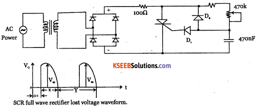
The SCR is connected with a diode bridge rectifier. The rectifier circuit converts AC to a unidirectional current through the thyristor. The voltage on the capacitor follows the diode rectifier waveform because RC circuit is connected to diode rectifier. During each half cycle when the voltage across the capacitor reaches trigger level which is just enough to supply gate trigger current to thyristor, then thyristor starts conducting. Firing angle \(\alpha=\left(\frac{x}{\mathrm{y}}\right)_{180}\)

![]()
Question 24.
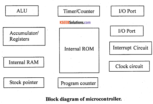
Draw the labelled block diagram of microcontroller.
Answer:
Question 25.
How do you represent.
(i) logical AND
(ii) logical OR
(iii) logical NOT operators in C programming?
Answer:
Internet is worldwide interconnection of millions of computers by means of complex network which serves as an inexpensive communication medium.
- Long-distance telephone and cable TV systems.
- To provide LAN connections.
- Closed-circuit TV systems used for security.
- Aircraft communication and controls.
Question 26.
What is internet? Write few applications of fibre optic communication system.
Answer:
Internet
- Using internet, access to required information is easy, economical, reliable and fast.
- With E-mail, messages reach destination with in minutes.
- E-mail can be sent and received from any place.
- Using E-mail, message can be sent to several persons simultaneously.
Applications
- Long-distance telephone and cable TV systems.
- To provide LAN connections.
- Closed-circuit TV systems used for security.
- Aircraft communication and controls.
Part – D
Answer any Three questions: 3 x 5 = 15
Question 27.
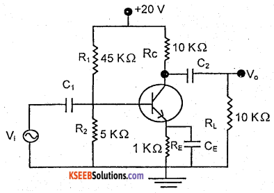
For the given CE amplifier circuit using silicon transistor. Calculate
i) Voltage across R2
ii) IE
iii) Zin(base)
iv) Zin (and)
v) Zo
Given \(\text { Given } r^{\prime} e=\frac{26 m V}{I_{E}}\) and β = 100
Answer:
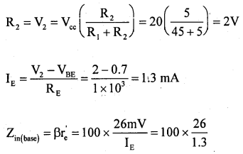
Zin = R1 || R2|| Zin(base) =1.38kΩ = 2kΩ
Zb =Rc || RL =(10kΩ) || (10kΩ) = 5kΩ
![]()
Question 28.
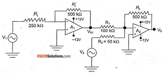
Calculate the output voltage if V1= 300mV and V2 = 700 mV in the following circuit.
Answer:

Question 29.
A Hortley oscillator oscillates at 15 KHz. If the capacitor in the tank circuit has a value of 0.01 pF and one of the inductors value is 1 mH, calculate the value of the other inductor.
Answer:

L1 + L2 = LT= 11.25 mH
L,1+ 1mH= 11.25mH, L1 = 10.25mH
Question 30.
A frequency modulated signal is given by 10sin[6 x 10⁸t + 5 sin 1250t].
Determine
i) Carrier frequency
ii) Modulating frequency
iii) Modulation index
iv) Maximum deviation
v) Carrier swing
Answer:
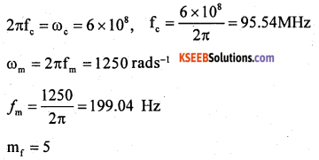
Maximum frequency deviation = δ= mf fm. = 5 x 199.04= 995.2 Hz
Carrier swing = 28 = 2(995.2) = 1990.4 Hz.
Question 31.
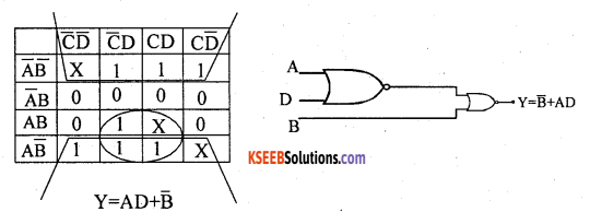
Simplify the Boolean expression Y = sm(l,2,3,8,9,11,13) + sd(0,10,15) using K-map. Draw the logic diagram using NAND-gates to realise the simplified expression.
Answer:
Part – E
Answer any Four questions. 4 x 5 = 20
Question 32.
Give the comparison between CB, CC and CE amplifiers on the performance characteristics.
Answer:
| Parameter | Types of Amplifiers. | ||
| CE | CB | CC | |
| Current gain | High (P) | Less than 1 | Highest (1+ p) |
| Voltage gain | High | Moderate | Low |
| Power gain | Highest | Moderate | Moderate |
| Phase shift | 180° | 0° | 0- |
| Input impedance | Moderate | Low | High |
| Output impedance | Moderate | High | Low |
| Bandwidth | Narrow | Wide | Wide |
| Applications | Used as AF amplifies | Used as RF amplifies | impedance matching |
![]()
Question 33.
What is a logarithmic amplifier? With circuit diagram, obtain an expression for output voltage of logarithmic amplifier using OP-amp.
Answer:
Answer:
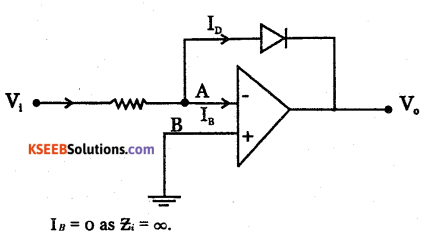
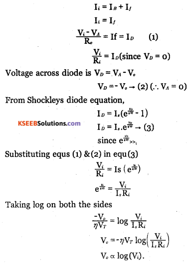
∴ The output voltage is proportional to natural logarithm of input voltage.
Question 34.
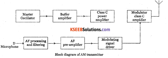
With a labelled block diagram, explain the working of AM transmitter.
Answer:
The transmitter performs modulation and raises the power level of a modulated wave to required level for effective radiation.
The microphone converts the audio signal into an equivalent audio electrical signal. The output is filtered to have a bandwidth of 10kHz.
The pre amplifier provides the required voltage amplification. The driver amplifier increases the power level of the signal as required by the high power modulation amplifier.
The high frequency carrier wave is generated by a crystal oscillator which has highest frequency stability. The Carrier signal is fed to a buffer amplifer which is a low gain, high input impedance amplifer which isolates crystal oscillator and the power level of the carrier signal to drive the modulated class C amplifier.
The modulating audio signal and carrier signal are applied to the modulator. The collector modulation is used for modulation in high power transmitter. The transmitting antenna transmits the signal.
Question 35.
Explain with circuit diagram and truth table, the working of clocked SR flip flop using NAND gates.
Answer:

It is constructed using inverters inserted into inputs of cross coupled NAND gates.
Working:
- When S=0, R=0, it does not respond and hence outputs Q and Q will remain in their previous state. This is called HOLD condition.
- When S=1 and R=0, the output Q and Q change to 1 and 0. This condition is called SET state.
- When S=0, R=1, the output Q and Q change to 0 and 1. This condition is called RESET state.
- When S=1 and R=l, it drives output Q and Q both to HIGH which is FORBIDDEN or INVALID condition.

![]()
Question 36.
Write an assembly language instructions to move 45H into register A and 5 EH into register R0. Then add them together and save the result in Rt. What is the content of R, after the execution of the program.
Answer:
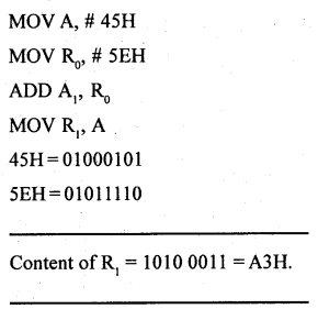
Question 37.
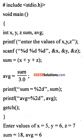
Write a C program to accept three integer and find their sum and average. Find the sum and average of 5, 6 and 7.
Answer:
